Product Details
Semiconductor Scrubber
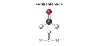
The fast growth in electronic industry has brought new environmental challenges for processes applied in manufacturing of semiconductor chips, which are important key part of many advanced electronic devices.Potentially hazardous chemicals; arsine, silane and phosphine are mainly used in fabrication of semiconductor by chemical vapor deposition (CVD).
Product Catalogue![]()
Description
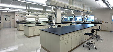
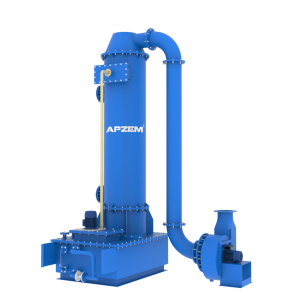
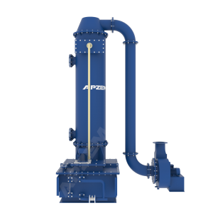
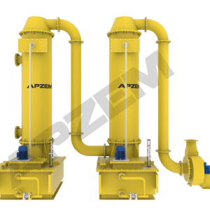
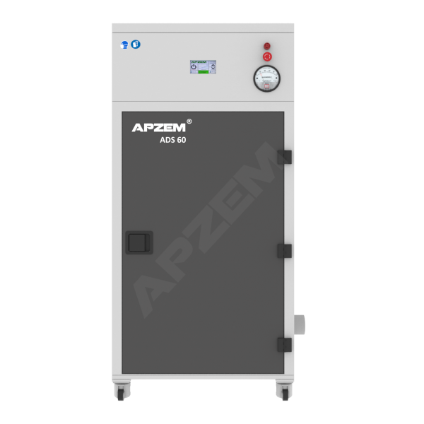
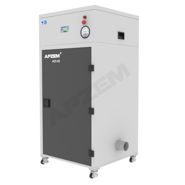
Single stage dust collector
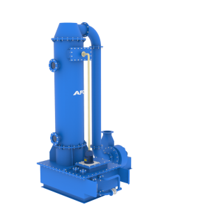
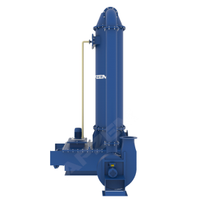
semiconductor scrubber
- The fast growth in electronic industry has brought new environmental challenges for processes applied in manufacturing of semiconductor chips, which are important key part of many advanced electronic devices.
- Potentially hazardous chemicals; arsine, silane and phosphine are mainly used in fabrication of semiconductor by chemical vapor deposition (CVD).
- Many large companies have improved facilities for handling and controlling the materials. However, small scale industries still are venting the by product gases into atmosphere directly. Increasing of production day by day, venting option is no longer is acceptable. There must be a regulation for controlling hazardous vapor containing silane, phosphine and arsine.
- We use state of the art cleaning technology to remove pollutants/contaminants that cause errors in semiconductor devices. It is designed considering to increase product yield, profitability and decrease the cost.
- Apzem developed a scrubber with innovative scrubbing material, which are specific in removing toxic gas emissions from semiconductor industry.
- Apzem semiconductor scrubber is smaller than conventional air pollution control equipment. Instead of installing a large equipment at outside of pant, our products can be placed at individual source. The scrubber convert the hazardous gases into simple non-toxic substances through chemical adsorption. Our products assist in eliminating toxic emissions and minimizing solid wastes from semiconductor fabrication plants.
Features of semiconductor scrubber
- Compact and Low weight
- Plug and play type
- Designed specially to capture fumes from semiconductor devices
- High efficiency more than 99 %
- Easy maintenance since there is no moving parts like wet scrubber
- Low energy consumption
- Does not require water and does not produce wastewater
- Can achieve PEL of OSHA standards
- Prevent re entrainment of pollutants in the laboratory
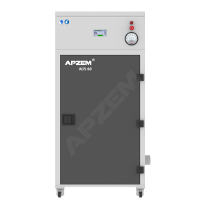
| Specifications | |
| Model No. | ADS-160 |
| Air Handling Volume | 400 CFM |
| Dimensions | 750 mm Length X 750 mm Width X 1650 mm Height |
| Material of Construction | §Carbon Steel
§Heavy Gauage §Fully Welded Cabinet §Anti corrosive coating |
| Removal Method | Chemical Adsorption |
| Filters | §Pre-filter
§Carbon filter |
| Removal Efficiency | §Above 99 % |
| Scrubber inlet port size | 100 mm dia. |
| Power Supply | 0.75 KW/ 1 HP
3 Phase |
| Noise level | Less than 75 dB |
https://www.apzem.in/index.php/product/semiconductor-scrubber/